ENIG (Electroless Nickel Immersion Gold) PCB
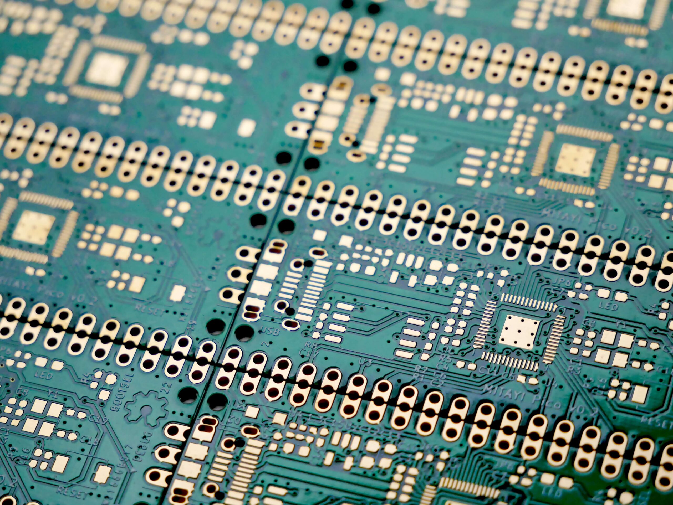
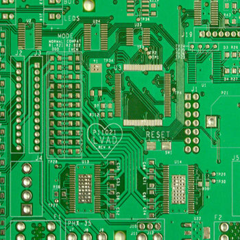
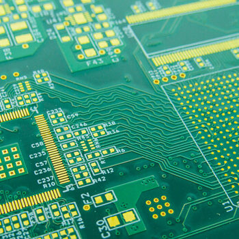
Electroless Nickel Immersion Gold (ENIG or ENi/IAu), also known as immersion gold (Au), chemical Ni/Au or soft gold, is a metal plating process used in the manufacture of printed circuit boards (PCBs), to avoid oxidation and improve the solderability of copper contacts and plated through-holes.
Technical Specification
PCB CAPABILITIES
| Specification | Standard |
|---|---|
| Maximum Board Size | 600mm X 520mm |
| Maximum Number Of Layer | 2 Layer (DSPTH) |
| Minimum Conductor Width | 4 mils (0.1mm) |
| Minimum Conductor Spacing | 4 mils (0.1mm) |
| Minimum Plated Hole Size | 8 mils (0.2mm) |
| Board Thickness Tloerence | 10% |
| Drill Tloerences | |
| 0.5 – 2.5mm | (+/-) 0.05mm |
| > 2.5mm | (+/-) 0.10mm |
| Size Tloerences | |
| < 150mm | (+/-) 0.10mm |
| > 150mm | (+/-) 0.20mm |
| Product Finish | |
| Surface Finish | HAL, TIN, Nickel, ENIG, Lead Free HAL |
| Copper Finish | 35μ, 70μ, 105μ |
| Solder Mask Finish | PISM |
| Solder Mask Colour | Green / White / Blue / Red / Black |
| Nickel Thickness | 120μ – 150μ |
| Gold Thickness | 5μ – 8μ |
| Legent Colour | White / Black / Yellow |
| Product Raw Material | |
| Singal Side | FR4, CEM1, MC PCB |
| Double Side | FR4, CEM-3 |
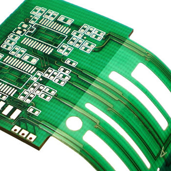
| Fixible | 0.2MM FR4, 0.1 polimide |
| Electrical Testing | |
| BBT, FPT | |
| Special Requirements | |
| Carbon Printing, Selective Gold, Selective Nickel |

